Interline transfer
The “Interline Transfer” matrix consists in a series of photodiodes separated by vertical transfer registers which are covered by an optical metallic shield (Fig. 11).
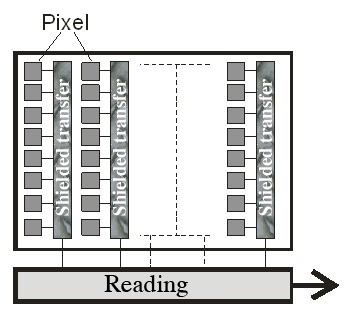
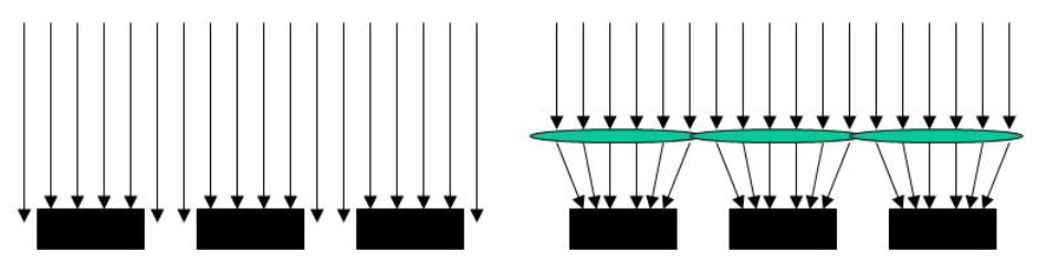
After integration, the charge generated by photodiodes is transferred to CCD vertical registers in about \(1\text{ }\mu\text{s}\) and so the smear is minimized. The main advantage of interline transfer is that the transfer from sensitive pixels to storage pixels is fast. So there is no need to shutter incident light. This is commonly known as "electronic shuttering". The disadvantage is that it lets less space to active sensors. The shield acts like a Venetian blind that darks half of the information present in the scene. The “area fill factor” can be as low as \(20\%\). (However, we can remedy to this by placing microlenses (Fig. 12) just in front of the sensor surface, in order to redirect the light toward sensitive cells. (HAD sensor: “Hole Accumulated Diode”).
Remarque :
For scenes in very high brightness, a portion of the incident light can still reach the vertical registers. For professional applications, we will then use a Frame Interline Transfer architecture, in which we find a shielded storage block under the active part as in the frame transfer.
As the interline systems are more often used in mass-produced camcorders, the design of the transfer registers is based on the standard video synchronization. With a \(2 :1\) interlacing system, each field is collected simultaneously and read alternately. It is called “frame integration”. In EIA 170 (formerly RS170), each field is read every \(1/50\text{s}\) (\(1/60\text{s US}\)). This allows a maximum integration time of \(1/25\text{ s}\) for each field.
Remarque :
The pseudo-interlacing system or field integration is obtained by changing the gate voltage; the centroid of the image is shifted of half a pixel in the vertical direction. It generates a \(50\%\) overlap between each field.
Complément :
The pixels have twice the standard size of interline transfer and hence a double sensitivity. However, it reduces the Modulation Transfer Function (MTF).
Microlenses
The optical fill factor may be inferior to \(100\%\) because of the manufacturing constraints of full frame systems. In the interline systems, the shielded storage area reduces the fill factor to less than \(20\%\). Microlens assemblies (also called microlens array or mini lens array) increase the effective optical fill factor (Fig.12). However, it will not reach \(100\%\) because of slight misalignment of the microlens system, of mini lens imperfections, non symmetrical shielded areas, and transmission losses.
Attention :
As the output voltage of the camera depends on the effective size of the sensor, increasing the fill factor with microlenses increases the effective size of the detector and the output voltage.